- HOME
- PRODUCTS
- SOLUTIONS
- SIRA Certified CCTV
- Mobile Attendance APP
- Payroll Software
- Attendance Management
- Cloud Attendance Solutions
- Access Control Management
- Automatic Parking Barrier
- User Activity Monitoring
- Employee Productivity
- Investigate Employees
- Deter Insider Threats
- Analytics & Monitoring
- Cyber Safety
- Cloud Anti-Virus Software
- COMPANY
- CONTACTS
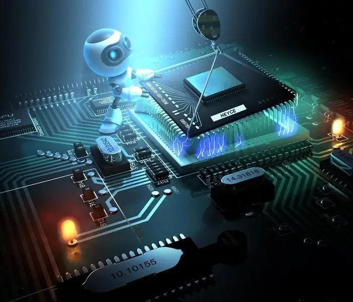
We at HEYCE are certain that apropos technology remains the most vital element & core fundamental to build products with optimum performance. With this belief, HEYCE incessantly invests into product research & development. This helps us achieve our goal to incorporate new and modern technology into our highly performing quality products & solutions. Our fully efficient and independent R & D is always on exhaustive knowledge building experiments to build future-proof & technologically advanced solutions applying information security technology as well as biometric verification sciences.
- Information Security Technology
- Intelligent 3D Face Recognition
- Forensic Fingerprint Sensor (OSSF)
- Biometric Verification Algorithm
- Biometric Identification Technology
Intelligent 3D Face Recognition
3-dimensional face recognition (3D face recognition) is a modality of facial recognition methods in which the three-dimensional geometry of the human face is used. It has been shown that 3D face recognition methods can achieve significantly higher accuracy than their 2D counterparts, rivalling fingerprint recognition.
3D face recognition has the potential to achieve better accuracy for biometric identification than its 2D counterpart by measuring geometry of rigid features on the face. This avoids such pitfalls of 2D face recognition algorithms as change in lighting, different facial expressions, make-up and head orientation. Another approach is to use the 3D model to improve accuracy of traditional image based biometric verification by transforming the head into a known view. Additionally, most range scanners acquire both a 3D mesh and the corresponding texture.
Capturing a real-time 3D image of a person's facial surface, 3D facial recognition uses distinctive features of the face -- where rigid tissue and bone is most apparent, such as the curves of the eye socket, nose and chin -- to biometrically identify the subject. These areas are all unique and don't change over time.
Using depth and an axis of measurement that is not affected by lighting, 3D facial recognition can even be used in darkness and has the ability to recognize a subject at different view angles with the potential to recognize up to 90 degrees (a face in profile).
Using the 3D software, the system goes through a series of steps for biometric identification of the identity of an individual.
3D face recognition finds applications across various industries, including security and surveillance, access control, identity verification, mobile devices, and augmented reality. Its versatility makes it suitable for a wide range of use cases, from securing facilities to enhancing user experiences in digital applications.
Biometric Capture
Acquiring an image can be accomplished by digitally scanning an existing photograph (2D) or by using a video image to acquire a live picture of a subject (3D).
Alignment
Once it detects a face, the system determines the head's position, size and pose. As stated earlier, the subject has the potential to be recognized up to 90 degrees, while with 2D, the head must be turned at least 35 degrees towards the camera for biometric identification.
Measurement
The system then measures the curves of the face on a sub-millimetre (or microwave) scale and creates a template.
representation
The system translates the template into a unique code. This coding gives each template a set of numbers to represent the features on a subject’s face.
Biometric Verification
If the image is 3D and the database contains 3D images, then matching will take place without any changes being made to the image. However, there is a challenge currently facing databases that are still in 2D images. 3D provides a live, moving variable subject being compared to a flat, stable image. New technology is addressing this challenge faced during biometric verification. When a 3D image is taken, different points (usually three) are identified. For example, the outside of the eye, the inside of the eye and the tip of the nose will be pulled out and measured. Once those measurements are in place, an algorithm (a step-by-step procedure) will be applied to the image to convert it to a 2D image. After conversion, the software will then compare the image with the 2D images in the database to find a potential match.
Biometric verification or identification
In biometric verification, an image is matched to only one image in the database (1:1). For example, an image taken of a subject may be matched to an image in the department of motor vehicles database to verify the subject is who he claims he is. If biometric identification is the goal, then the image is compared to all images in the database resulting in a score for each potential match (1: n). In this instance, you may take an image and compare it to a database of mugshots to identify who the subject is
Forensic Fingerprint Sensor (OSSF)
Sensor Technology
All fingerprint systems manufactured by Heyce Technologies incorporate a forensic science based sensors utilizing a technology known as optic sensor over semiconductor film –OSSF (prism method). This technology based sensors verify using 7 different checks to ascertain if the fingerprint is live. This makes forging or security breach impossible.
Modus of Operandi (OSSF)
Disposing the light absorption layer formed in contact with a poly-crystal silicon layer of a bottom gate type poly-crystal silicon TFT allows a depletion layer formed between drain and channel forming regions to extend further into the inside of the light absorption layer, resulting in collection of photo carriers produced in the depletion layer into the channel forming region. The photo carriers collected into the channel forming region are subsequently collected into the source region to be output as large photocurrents by high mobility of the poly-crystal silicon.
Gate Electrode
Linear Image sensor
The Technology
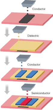
The image sensor comprises of a linear image sensor which consists of a gate electrode over a poly-crystal semiconductor layer(substrate) formed over the gate electrode with a gate insulating film interposed between and an amorphous semiconductor layer formed on the poly-crystal semiconductor layer. A thin film transistor is electrically connected to said optical sensor in series with a capacitor having a first and a second electrode.
The first electrode of this capacitor is electrically connected to optical sensor and thin film transistor. The gate electrode of the thin film transistor is electrically connected to a shift register circuit. The linear image sensor of is amplified and electrically connected to a signal output terminal.
Background of The Invention
The present invention relates to an optical sensor comprising an amorphous silicon layer with a greater light absorption coefficient for visible light to produce photo carriers for use as a photo current to be transmitted via highly mobile poly-crystal silicon. More specifically, the present invention relates to an optical sensor comprising an amorphous silicon layer formed to bring into contact with a channel forming region of a bottom gate-type poly-crystal silicon thin film transistor.
Summary of The Invention
The present invention has been made in view of the above, and the present invention provides an entirely novel structure with a higher level of photosensitivity and operation rate by skillfully combining excellent absorption performance of amorphous silicon and high mobility of poly-crystal silicon.
In other words, in an optical sensor according to the present invention, a photo-detector portion using an amorphous silicon layer is arranged in contact with the upper portion of a poly-crystal silicon TFT, a depletion layer at the source or drain portion of the poly-crystal silicon TFT is extended to the interior of the amorphous silicon layer, and photo-carriers produced by absorption by the amorphous silicon layer are possible to be swiftly transmitted to poly-crystal silicon.
An object of the present invention is to provide an entirely novel optical sensor by combining excellent properties of the two materials, i.e., photosensitivity for visible radiation of amorphous silicon and high mobility of poly-crystal silicon.
In addition, the light in short wavelength region easily realized a structure in which the photo carriers are produced not in the amorphous silicon layer but directly in a channel forming region of the poly-crystal silicon. Therefore, the present invention has another object to provide a highly sensitive optical sensor to cover all of the visible radiation ranges of blue, green, and red.
OSSF Fingerprint sensors have the following advantages over other fingerprint sensors
- No direct contact with sensor film & Prism
- Increased life of sensor
- Improved fingerprint detection for wet and scaled fingerprints
- Scratch proof sensor surface
- 100% Moisture resistant sensor
- Advanced Encryption Standard
- Accurate Fingerprint Matching
Technical Specification: Fingerprint Sensor
- Pixel resolution: 850 dpi (average X,Y over the field)
- Scan capture area: 18 mm (nom. width at center), 20 mm (nom. length)
- 8-bit grayscale (256 levels of gray)
- Reader size (approximate):63 mm x 39 mm x 9.1 mm
- Supply Voltage: 5.0V ±5%
- Supply Current – scanning 190 mA (Typical)
- Supply Current – idle mode 140 mA (Typical)
- Supply Current – suspend mode 1.5 mA (Maximum)
- ESD Susceptibility & >15 kV, mounted in case
- Temperature, Operating :0°C - 53° C
- Humidity, Operating: 20% - 92% non-condensing
- Temperature, Storage: -19° - 60° C
- Humidity, Storage: 20% - 95% non-condensing
- Scan data: 8-bit grayscale
- Standards Compliance: FCC Class B, CE, ICES, BSMI, MIC, USB, WHQL ECCB-954 / RoHS
Integrated Smart Card
A contactless smart card is in any pocket-sized card with embedded integrated circuits which can process and store data. This implies that it can receive input which is processed and delivered as an output via radio frequencies. There are two broad categories of contactless smart cards. Memory cards contain non-volatile memory storage components, and perhaps some specific security logic. Contrary to popular belief contactless smart cards do not contain an ordinary read-only RFID, but they do contain a re-writable smart card microchip that can be transcribed via radio frequencies. A contactless smart card is in any pocket-sized card with embedded integrated circuits which can process and store data. This implies that it can receive input which is processed and delivered as an output via radio frequencies. There are two broad categories of contactless smart cards. Memory cards contain non-volatile memory storage components, and perhaps some specific security logic. Contrary to popular belief contactless smart cards do not contain an ordinary read-only RFID, but they do contain a re-writable smart card microchip that can be transcribed via radio frequencies.
Data Encryption
Often there has been a need to protect information from snooping eyes. In the electronic age, information that could otherwise benefit a group or individual can also be used against such groups or individuals. Industrial espionage among highly competitive businesses often requires that extensive security measures be put into place. In capture of human recognition data, it becomes even more essential to protect and preserve the data and all related transmission.
Traditionally, several methods can be used to encrypt data streams, all of which can easily be implemented through software, but not so easily decrypted when either the original or its encrypted data stream are unavailable. The best encryption methods have little effect on system performance, and may contain other benefits (such as data compression) built in. The well-known utility offers both compression AND data encryption in this manner. Also DBMS packages have often included some kind of encryption scheme so that a standard file copy & cannot be used to read sensitive information that might otherwise require some kind of password to access. They also need high performance methods to encode and decode the data.
Encryption Used (AES – Advanced Encryption Standard)
Word/byte rotation and XOR bit masking. If you rotate the words or bytes within a data stream, using multiple and variable direction and duration of rotation, in an easily reproducible pattern, you can quickly encode a stream of data with a method that is nearly impossible to break. Further, if you use an XOR mask in combination with this (the bits in certain positions from 1 to 0, or 0 to 1) you end up making the code breaking process even more difficult. The best combination would also use pseudo random effects, the easiest of which would involve a simple sequence like Fibonacci numbers. The sequence 1,1,2,3,5,...is easily generated by adding the previous 2 numbers in the sequence to get the next. Doing modular arithmetic on the result (i.e. Fib. sequence mod 3 to get rotation factor) and operating on multiple byte sequences (using a prime number of bytes for rotation is usually a good guideline) will make the code breaker job even more difficult, adding the pseudo-random effect that is easily reproduced by your decryption program. In some cases, you may want to detect whether data has been tampered with, and encrypt some kind ofchecksum into the data stream itself. An intrusion that infects such aprotected program would no doubt neglect the encryption algorithm and authorization/checksum signature. The program could then check itself each time it loads, and thus detect the presence of file corruption. A cyclic redundancy check is one typically used checksum method. It uses bit rotation and an XOR mask to generate a 16-bit or 32-bit value for a data stream, such that one missing bit or 2 interchanged bits are more or less guaranteed to cause achecksum error. This method has been used for file transfers for a long time, such as with XMODEM-CRC. The method is somewhat well documented, and standard. But, a deviation from the standard CRC method might be useful for the purpose of detecting a problem in an encrypted data stream, or within a program file that checks itself for viruses.
Fingerprint Recognition Algorithm
Core Detection
This step is to detect the core of the registered fingerprint image f(n1, n2) and the input fingerprint image g(n1, n2) in order to align the displacement between the two images. The core is defined as a singular point in a fingerprint image that exhibits the maximum ridge line curvature. The Poincar´e index method [6] is used to detect the core in our system.
Displacement and rotation alignment
We need to normalize the displacement and the rotation between the registered fingerprint f(n1, n2) and the input fingerprint g(n1, n2) in order to perform the high-accuracy fingerprint matching.
In the case when both fingerprint images have their cores,we first align the translation al displacement between fingerprint images using the position of the cores. Next, we normalize the rotation by using a straightforward approach as follows. We first generate a set of rotated images fθ(n1, n2) of the registered fingerprint f(n1, n2) over the angular range −40◦ ≤ θ ≤ 40◦ with an angle spacing 1◦, where bi-cubic interpolation is employed for image rotation. The rotation angle Θ of the input image relative to the registered image can be determined by evaluating the similarity between the rotated replicas of the registered image fθ(n1, n2) (−40◦ ≤ θ ≤ 40◦) and the input image g(n1, n2) using the BLPOC function. When either f(n1, n2) or g(n1, n2) does not have its core, we first normalize the rotation by the above straightforward approach. Next, we align the translational displacement between the rotation-normalized image fΘ(n1, n2) and the input image g(n1, n2). The displacement can be obtained as the peak location of the POC function between fΘ(n1, n2) and g(n1, n2). Thus, we have normalized versions of the registered image and the input image, which are denoted by f _(n1, n2) and g_(n1, n2).
Common region extraction
Next step is to extract the overlapped region (intersection) of the two images f _(n1, n2) and g_(n1, n2). This process improves the accuracy of fingerprint matching, since the non over lapped areas of the two images become the uncorrelated noise components in the BLPOC function. In order to detect the effective fingerprint areas in the registered image f _(n1, n2) and the input image g_(n1, n2), we examine the n1-axis projection and the n2-axis projection of pixel values. Only the common effective image areas, f __(n1, n2) and g__(n1, n2), with the same size are extracted for the succeeding image matching step.
Fingerprint matching
We calculate the BLPOC function rK1K2f__g__ (n1, n2) between the two extracted images f __(n1, n2) and g__(n1, n2), and evaluate the matching score. The BLPOC function may give multiple correlation peaks due to elastic fingerprint deformation. Thus, we define the matching score between the two images as the sum of the highest two peaks of the BLPOC function rK1K2f__g__ (n1, n2).
Experimental Results
This section describes a set of experiments for evaluating fingerprint matching performance of the proposed algorithm. In our experiment, the database consists of impressions obtained from 30 subjects using a pressure sensitive sensor (BLP-100, BMF Corporation), which can capture fingerprint images of 256 × 384 pixels. In the captured images, 20 of subjects have good-quality fingerprints and the remaining 10 subjects have low-quality fingerprints due to dry fingertips (6 subjects), rough fingertips (2 subjects) and allergic-skin fingertips (2 subjects).
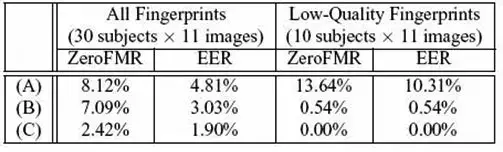
Figure 3 shows some examples of fingerprint images Thus, the test set considered here is specially designed to evaluate the performance of fingerprint matching under difficult condition. We capture 11 impressions of the right index finger for every subject, each of which is taken at different timing. The total number of fingerprint images used in this experiment is 330 (30 subjects × 11 images). We compare three different matching algorithms: (A) a typical minutiae-based algorithm (which is commercially available), (B) a simple POC-based algorithm [5], and (C) the proposed algorithm. The performance of the biometrics-based identification system is evaluated by the Receiver Operating Characteristic (ROC) curve, which illustrates the False Non- Matching Rate (FNMR) against the False Matching Rate (FMR) at different thresholds on the matching score. We first evaluate the FNMR for all possible combinations of genuine attempts; the number of attempts is 11C2 × 30 = 1650. Next, we evaluate the FMR for 30C2 = 435 impostor attempts, where we select a single image (the first image) for each fingerprint and make all the possible combinations of impostor attempts. Figure 4 shows the ROC curve for the three algorithms (A)–(C). The proposed algorithm (C) exhibits significantly higher performance, since its ROC curve is located at lower FMR/FNMR region than those of the minutiae-based algorithm (A) and the POC-based algorithm (B). The Equal Error Rate (EER) and the Zero FMR are used to summarize the accuracy of a verification system. The EER is defined as the error rate where the FNMR and the FMR are equal. The ZeroFMR is defined as the lowest FNMR where FMR=0%. Table I summarizes EER and ZeroFMR for matching attempts using all the fingerprints and for attempts using only low-quality fingerprints. In the case of using all the fingerprints, the EER of the proposed algorithm (C) is 1.90%, while the EER of the POC-based algorithm (B) is 3.03%.
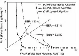
TABLE I. ZeroFMR and EER for matching attempts using all the fingerprints and for matching attempts using only lowquality fingerprints.
S3C44B0X (ARM7TDMI) CPU core Processor: (HT BA-30C, HT SL)
Fingerprint Processor
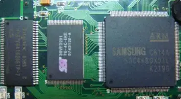
S3C44B0X 16/32-bit RISC microprocessor
Samsungs S3C44B0x processor is based on a 16/32-bit ARM7TDMI RISC core. The architectural enhancements of ARM7TDMI include the Thumb decompresser, on-chip ICE-breaker debug support and a 32-bit hardware multiplier. The processor card takes full advantage of the integrated on-chip functions and the peripherals of the S3C44B0x. The card is connected to a carrier board via a 200-pin DIMM socket The 16-bit data bus, I/O and all other hardware interfaces are extended to the DIMM.
S3C44B0x Processor Features
- Samsung S3C44B0x microcontroller based on a 2.5V Static ARM7TDMI CPU core with 8 KB cache and 8 MByte SDRAM
- 2 MByte NOR Flash
- 5-ch PWM timers & amp; 1-ch internal timer
- Watchdog Timer
- 71 general purpose I/O ports / 8-ch external interrupt source
- On-chip PLL generates the 8 MHz OSC to operate the MCU at up to 66 MHz
- 32.768 kHz Real-Time clock
- JTAG interface
- 16-bit data bus, I/O and all other hardware interface expansions via DIMM 200-pin
- RTC with calendar function.
- Single 3.3V power supply
- Temperature Range: 0 to +70 Celsius
ARM922T Processor (HTPRO, HT G-35, HT FC-35, HT CC-35)
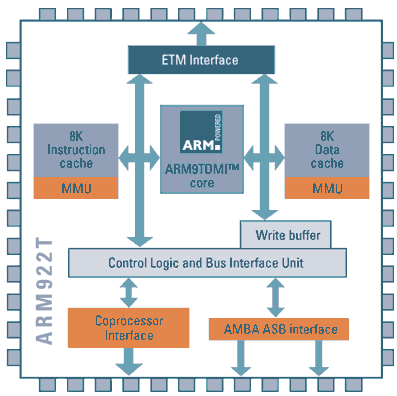
Based on the most widely adopted embedded RISC architecture, the ARM922T embedded processor PLDs provides single chip-integration of a high-performance 200 MHz ARM922T processor core, programmable logic, on-chip memory, and key peripherals. This integration of leading edge technology provides embedded system designers a reduction in overall development cost and accelerated time-to-market versus ASIC solutions. The integration also affords performance and board space advantages over conventional designs that use multiple discrete components
Combining logic, memory, and a processor core, Alteras Excalibur embedded processor solutions support to integrate an entire system on a single PLD. The Nios soft core embedded processor and the ARM-based hard core embedded processor offer the flexibility of processor cores with the integration of an SOPC solution. ARM922T processors support up to 38,400 logic elements (1,000,000 gates). They offer full integration with APEX PLD architecture, and are supported by the Quartus II development tool, which is optimized for the ARM922T embedded processor families.
Based on the most widely adopted embedded RISC architecture, the ARM922T embedded processor PLDs provides single chip-integration of a high-performance 200 MHz ARM922T processor core, programmable logic, on-chip memory, and key peripherals. This integration of leading edge technology provides embedded system designers a reduction in overall development cost and accelerated time-to-market versus ASIC solutions. The integration also affords performance and board space advantages over conventional designs that use multiple discrete components.